2021. Review article in SID's Information Display magazine covering Mattrix Technologies.
2011. Intrinsic nonuniformity in the polycrystalline-silicon backplane transistors of active matrix organic light-emitting diode displays severely limits display size. Organic semiconductors might provide an alternative, but their mobility remains too low to be useful in the conventional thin-film transistor design. Here we demonstrate an organic channel light-emitting transistor operating at low voltage, with low power dissipation, and high aperture ratio, in the three primary colors. The high level of performance is enabled by a single-wall carbon nanotube network source electrode that permits integration of the drive transistor and the light emitter into an efficient single stacked device. The performance demonstrated is comparable to that of polycrystalline-silicon backplane transistor-driven display pixels.
2008. By experiment and supporting theory we demonstrate the facile modulation of the electronic contact-barrier across the junction between single wall carbon nanotubes (SWNTs) and two distinct organic semiconductors demonstrating a new realm of application for carbon nanotubes. We exploit this ability to enable two devices: a vertical field-effect transistor and a vertical light-emitting transistor. The vertical architec- ture, which is readily facilitated by the specific properties of the nanotubes, allows the use of low mobility semiconductors that would otherwise be considered unsuitable for field effect transistors, thereby expanding the range of potential active materials. For the light-emitting transistor the gate control should permit new pixel drive schemes and affords the potential for increased device lifetimes.
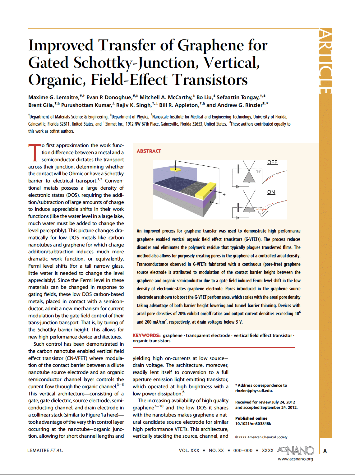
2012. An improved process for graphene transfer was used to demonstrate high performance graphene enabled vertical organic field effect transistors (G-VFETs). The process reduces disorder and eliminates the polymeric residue that typically plagues transferred films. The method also allows for purposely creating pores in the graphene of a controlled areal density. Transconductance observed in G-VFETs fabricated with a continuous (pore-free) graphene source electrode is attributed to modulation of the contact barrier height between the graphene and organic semiconductor due to a gate field induced Fermi level shift in the low density of electronic-states graphene electrode. Pores introduced in the graphene source electrode are shown to boost the G-VFET performance, which scales with the areal pore density taking advantage of both barrier height lowering and tunnel barrier thinning. Devices with areal pore densities of 20% exhibit on/off ratios and output current densities exceeding 106 and 200 mA/cm2, respectively, at drain voltages below 5 V.
2017. The carbon nanotube enabled vertical field effect transistor technology further demonstrates its promise to allow cost effective manufacturing of large screen AMOLED displays. Formed essentially by directly stacking an OLED onto the vertical channel layer of the vertical field effect transistor, the resulting vertical organic light emitting transistor combines the driving transistor, storage capacitor and light emitter into a single integrated device. A QVGA AMOLED prototype using this technology was demonstrated at the 2016 San Francisco SID Display Week, winning the I-Zone award for best prototype.
2010. State-of-the-art performance is demonstrated from a carbon nanotube enabled vertical field effect transistor using an organic channel material. The device exhibits an on/off current ratio >105 for a gate voltage range of 4 V with a current density output exceeding 50 mA/cm2. The architecture enables submicrometer channel lengths while avoiding high-resolution patterning. The ability to drive high currents and inexpensive fabrication may provide the solution for the so-called OLED backplane problem.
2004. We describe a simple process for the fabrication of ultrathin, transparent, optically homogeneous, electrically conducting films of pure single-walled carbon nanotubes and the transfer of those films to various substrates. For equivalent sheet resistance, the films exhibit optical transmittance com- parable to that of commercial indium tin oxide in the visible spectrum, but far superior transmittance in the technologically relevant 2- to 5-micro- meter infrared spectral band. These characteristics indicate broad applica- bility of the films for electrical coupling in photonic devices. In an example application, the films are used to construct an electric field–activated optical modulator, which constitutes an optical analog to the nanotube-based field effect transistor.
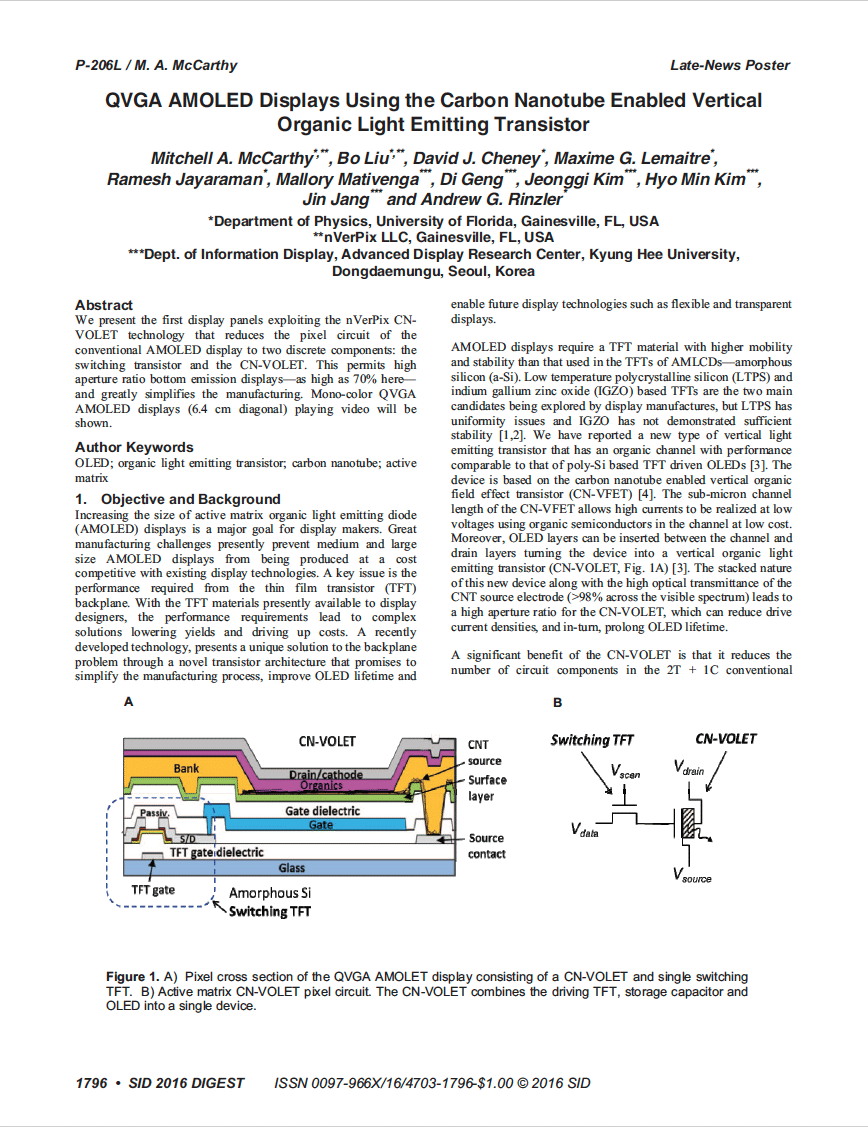
2016. We present the first display panels exploiting the nVerPix CNVOLET technology that reduces the pixel circuit of the conventional AMOLED display to two discrete components: the switching transistor and the CN-VOLET. This permits high aperture ratio bottom emission displays—as high as 70% here— and greatly simplifies the manufacturing. Mono-color QVGA AMOLED displays (6.4 cm diagonal) playing video will be shown.
The scaling behavior of carbon nanotube (CNT)-organic semiconductor heterojunction enabled vertical field effect transistors are comprehensively examined by two-dimensional consistent device simulations. Tunneling current is modeled by introducing tunneling induced carrier generation into the current continuity equation. Modulation of both the CNT-semiconductor Shottky barrier height and thickness are examined. The tunneling current and thermionic current dominate at on-state and off-state, respectively. Barrier height modulation plays an important role and improves the on-off current ratio and sub-threshold swing considerably. Small diameter CNT is preferred for enhancing the gate control on the CNT-channel barrier height. Reducing the effective gate oxide thickness by either a thin oxide or a high-j gate insulator gives improvement of device performance, but the former one works more efficiently. The channel length and CNT spacing should be carefully engineered due to the trade-off between device characteristics in the sub-threshold and above threshold region.